This is the second update from our team of interns, comprised of four University of Cambridge undergrads. Their work is kindly sponsored by IMC Financial Markets who are also helping to advise this summer project.
At the time of our last blog post, we had just finished VGA and were working on implementing the frame buffer. Over the last 2 weeks, we have made significant progress, completing the frame buffer and starting video decode.
The frame buffer was developed iteratively. Initially, it was a small Block RAM attached to the SoC’s AXI-Lite bus. This was useful for creating a prototype, but its limited size lead to it being replaced with an in-memory frame buffer, supplemented with a BRAM line buffer. The end result is shown below, the component is connected to the TileLink bus.

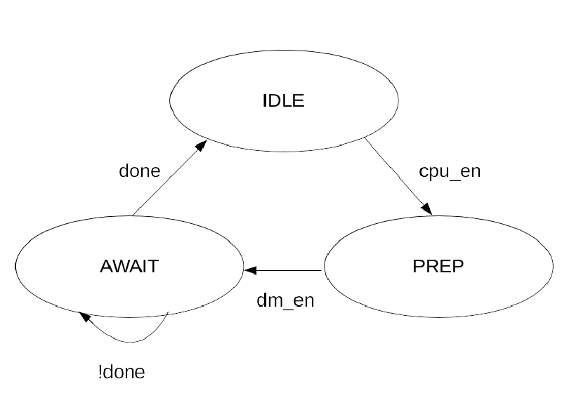
This component builds on the VGA controller, for which documentation will be added shortly. We have added a data mover (a unidirectional DMA), to move data from the in memory frame buffer into the local video memory. The video memory acts as a line buffer, the data mover (DM) moves one line from the in-memory frame buffer at a time. Meanwhile the VGA controller flushes the new lines to the screen, displaying the image from memory. The DM obeys the state machine shown in the diagram below. The DM Controller is memory mapped, allowing the CPU to communicate with it. Currently, it can only accept one request at a time, further requests are ignored until the component moves back to the IDLE step. Requests consist of source and destination addresses, and a length. A planned extension is adding a FIFO queue to the controller to allow multiple requests to be supported.

The decision was made to implement a unidirectional data mover over a more complex and capable bidirectional DMA component as only unidirectional movement was needed for now. Later on, we will need bidirectional access as the video accelerator will need to write back to memory. We hope to enable bidirectionality by simply duplicating the existing unidirectional design.
Our next tasks relate to video decoding. We will be adapting a reference MPEG-2 codec to decode video on the FPGA and adding extra components to the SoC design to improve the performance of the codec, such as DCT and iDCT accelerators.
Contact us
lowRISC is a not-for-profit company using collaborative engineering to develop and maintain open source silicon designs and tools, through a unique combination of skills, expertise and vision.
We provide a home for multi-partner projects that deliver verified, high quality IP and tools, which provide the solid foundations that are necessary for the rapid development cycles required for next generation silicon products. lowRISC employs an engineering team in Cambridge, UK, working on our own developments, partner projects, and work-for-hire that is aligned with our mission.